

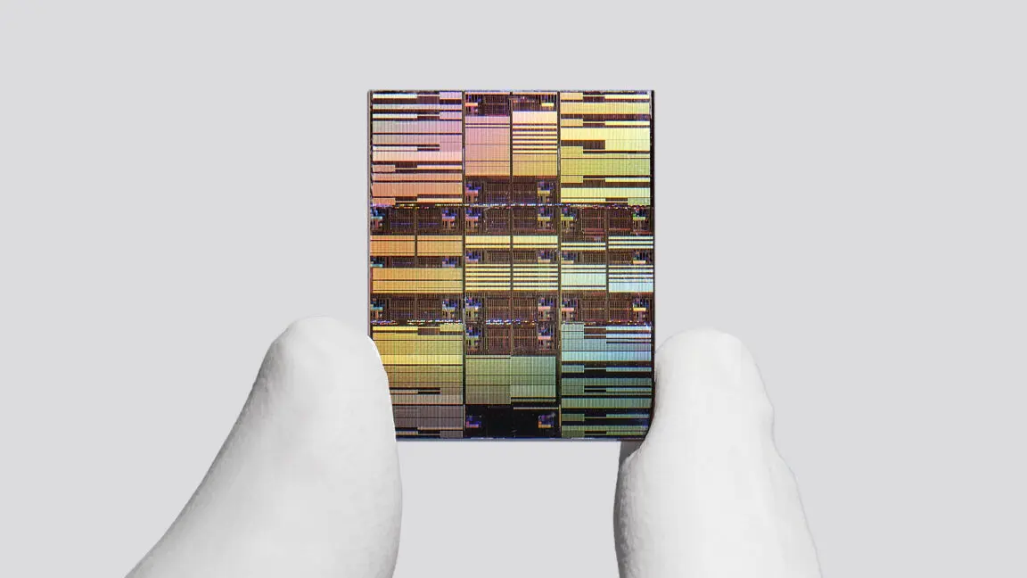
A new chip architecture from IBM can integrate nearly 100 billion transistors on a chip the size of a human fingernail, nearly doubling the transistor density of its previous generation. The resulting boost in compute performance and energy efficiency comes from what IBM describes as the world's first sub-1 nanometer chip technology for AI data centers.
"It's not just an incremental step, it's a meaningful leap forward," said Jay Gambetta, director of IBM Research and IBM Fellow, during an advance media briefing. He described the new technology as "pointing to a future where computing becomes significantly more powerful without a corresponding increase in energy."
To understand what "sub-1 nanometer" means, it helps to know that building functional chips with physical features smaller than 1 nanometer is impractical due to quantum tunneling and other limitations. Instead, IBM is claiming that its new nanostack architecture delivers the performance improvements one would expect from a theoretical chip with features smaller than 1 nanometer. Specifically, IBM calls this the 0.7-nanometer node, or 7 angstrom node (since 1 nanometer equals 10 angstroms).
Node numbers no longer correspond to actual physical dimensions. In the 1970s and 1980s, nodes like 180 nanometers matched the size of chip features, but for decades that correlation has disappeared. Modern nodes are marketing labels that represent a generation of technology with certain performance and density targets. For example, TSMC's 3nm and 2nm processes do not have literal 3nm or 2nm features. IBM's 0.7nm claim is similarly a shorthand for the expected performance gains, not the actual gate length.
How the nanostack architecture works
To overcome physical scaling limits, IBM's nanostack architecture vertically stacks transistors in a staggered layout. This packs more transistors into the same chip area. The architecture builds on IBM's earlier development of nanosheet transistors, which paved the way for its 2nm node introduced in 2021.
The basic unit consists of two transistors stacked and bonded together. Each transistor comprises three nanosheets individually 5 nanometers thick (about 15 rows of silicon atoms), with a 9-nanometer gap between each nanosheet. This vertical stacking, combined with the staggered arrangement, dramatically increases transistor density without shrinking individual features.
This approach is necessary because traditional planar scaling has hit a wall. As transistor dimensions approach atomic scales, leakage currents and heat dissipation become unmanageable. FinFET transistors, which were the industry standard for a decade, are giving way to nanosheet designs that allow better electrostatic control. IBM's nanostack takes that further by adding a third dimension.
Performance gains for the AI era
According to IBM's published technical reports, the nanostack architecture could deliver 50% higher computing performance or 70% greater energy efficiency compared to its 2nm node chips. These figures are critical for AI workloads, which require massive parallel processing and memory bandwidth. The company presented the technology at the 2025 IEEE Symposium on VLSI Technology and Circuits in Kyoto, Japan.
IBM researchers also demonstrated a 40% improvement in scaling for static random-access memory (SRAM), which is essential for fast, energy-intensive read and write operations in AI applications. This improvement is achieved through a staggered-channel design for SRAM bit cells—each containing six transistors—that reduces overall cell height by 40%, allowing more SRAM to fit in the same space.
This is particularly significant because SRAM scaling has slowed in recent generations. Gambetta noted that SRAM scaling improved only a few percent between the 3nm and 2nm nodes. "This achievement of 40% will eventually industrialize itself in AI workflows, which require higher bandwidth and high efficiency," he said.
AI models like large language models and recommendation systems rely heavily on SRAM for caching weights and intermediate data. Faster, more energy-efficient SRAM directly translates to lower latency and reduced power consumption in data centers, which are already straining electrical grids.
The roadmap for sub-1 nanometer nodes
IBM does not manufacture commercial chips; it is a research organization that collaborates with semiconductor firms like Rapidus in Japan and Samsung in South Korea. For its previous 2nm nanosheet architecture, IBM partnered with Rapidus to bring it to mass production. The company declined to name specific partners for the new sub-1nm technology, but Huiming Bu, vice president of IBM Semiconductors Global R&D, expects commercial chips using the nanostack architecture could enter production within five to ten years.
Other companies have already built on IBM's nanosheet work. TSMC independently developed nanosheet transistors for its 2nm node. "Nanosheet has become the foundation of the next generation of transistor scaling," Bu said. "Today, nanosheet is adopted by all leading foundries for most of the 3nm chips and all of the 2nm chips."
Bu predicted that nanostack will follow the same pattern: "It will replace nanosheet as today's mainstream in leading foundries, whether it's CPUs or GPUs. Within a decade, this will become another mainstream that we have invented and helped industry to transform."
The timeline is ambitious. Achieving sub-1nm nodes requires new materials (such as high-mobility channels like germanium or 2D materials), advanced lithography (likely high-NA EUV), and novel integration techniques. IBM's nanostack addresses the structural challenge, but manufacturing at scale will require significant investment and process maturity. If successful, the technology could extend Moore's Law well into the next decade, enabling exascale AI computing and possibly new applications in quantum-classical hybrid systems.
For now, IBM has demonstrated a working prototype at the VLSI symposium. The industry will be watching to see whether Rapidus or another partner can bring this to volume production. With AI demand surging, any improvement in compute density and energy efficiency is welcome—and IBM's nanostack architecture may be the next big leap.
Source: Ars Technica News